HomeCurrent Research – Low Temperature Scanning Probe Microscopy
Current Research – Low Temperature Scanning Probe Microscopy
A local probe to help detect various forces (e.g. van der Waals, electrostatic, magnetic, etc.) at the nanometer scale is a powerful tool in understanding the fundamental properties of systems with relevant mesoscopic length scales. Such systems include 1) complex oxides, where for many materials there are local inhomogeneities in the electron density and other order parameters of the system and 2) hybrid mesoscopic structures incorporating different material types such as normal metals, ferromagnets and superconductors. Both of these systems have been extensively studied in our group (see other projects here), principally by means of electrical transport measurements.
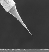
Figure 1. Etched tungsten tip
In order to study these systems on a local level we are developing a low temperature scanning probe microscope (LTSPM) based on a tuning fork transducer to operate at millikelvin temperatures. This LTSPM will be capable of performing magnetic force microscopy (MFM) and electrostatic force microscopy (EFM) in addition to atomic force microscopy (AFM). With a little change in outside electronics, the same setup can also be configured to perform scanning tunneling microscopy (STM).
As a conventional AFM, which acquires images by bouncing a laser off a scanning cantilever, dissipates too much heat and is too cumbersome, our AFM design is based on quartz tuning forks like those found in most watches. These tuning forks have a very sharp resonance (Q = 10000) at around 32 kHz. Excited at this frequency, the tuning fork is lowered toward the sample surface until a tip attached to one of the fork’s tines begins to interact with the sample surface. These force interactions slightly shift the resonance peak of the tuning fork. By scanning the tip and fork across the sample surface and tracking the resonance shifts an image of the sample topography can be produced. The power dissipation with this tuning fork transducer is much less than with other techniques (such as laser deflection), making it suitable for operation at millikelvin temperatures. With adjustments to the type of tip, and some signal processing one can also do MFM, EFM and STM on samples.
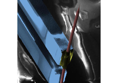
Figure 2. Quartz tuning fork with an attached etched tungsten wire, used as a force transducer in our home-built scanning probe microscope.
We use tips made from etched tungsten (W) wire as our local probe. The etching procedure fabricates tips with diameters of the order of 10-20 nm. Figure 1 shows an SEM image of an etched tip. The etched tip is attached to the tine of a tuning fork using super-glue, and the tuning fork is ready to be used as an AFM probe. Figure 2 shows a false colour SEM image of an etched W wire attached to the tuning fork. The tuning fork is shaded blue, the super glue is green and the W wire is in red. The W wire is also electrically connected at the other end, giving us the ability to apply an electrical voltage to the tip, enabling the probe to perform EFM. We are currently developing etching Ni wire to make probes for MFM measurements.
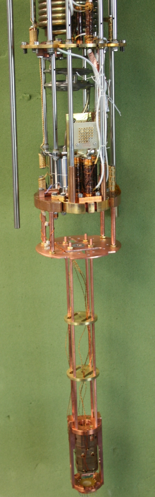
Figure 3 shows the dilution fridge (MX100 from Oxford) on which the positioner and scanner of the LTSPM is attached. The positioner and scanner piezo based and acquired from Attocube systems, AG. We have employed a number of acoustic and electrical noise isolating techniques, in order to get the best sensitivity and resolution from our LTSPM. Most of the electronics and the software to control the LTSPM has been developed in-house, giving us the flexibility to easily modify the setup to perform different types of microscopies (e.g. STM, SKPM, SHPM, etc).
Figure 3. LTSPM mounted on the mixing chamber of a dilution refrigerator.
We are currently developing a microwave impedance microscope (MIM) based on a tuning fork transducer. This enables noncontact imaging of the conductivity of a sample even well below the surface by measuring the complex impedance of a scanning probe tip at microwave frequencies as it scans across a sample. Commercial MIMs use a specially designed cantilevers with built-in coplanar waveguides to do these measurements. However, it has been shown that one can use a tuning fork with an etched wire tip similar to that shown in Fig. 2 if one uses an appropriate impedance matching circuit. We have implemented a Mach-Zehnder interferometer matching circuit to greatly increase the sensitivity of the instrument. Figure 4 shows simultaneously taken topographic (a) and MIM (b) images of an “aged” Au metal film on an oxidized Si substrate. While the topographic image of the Au film looks relatively smooth, the MIM image shows it has strong modulations in its conductivity. MIM is thus a powerful tool to study nanometer scale variations in the conductivity of samples and devices.
Figure 4. Simultaneous topographic (a) and MIM images of a gold film on an oxidized Si substrate.